Model I (Without an Adapter)
In the olden days, when 2732 EPROMs still were manufactured, flashing a new ROM for the Model I was easier. Since that is no longer an option, and there is no direct replacement for the TRS-80 ROMs anymore, people have been writing up methods to use a modern 27C256 EPROM.
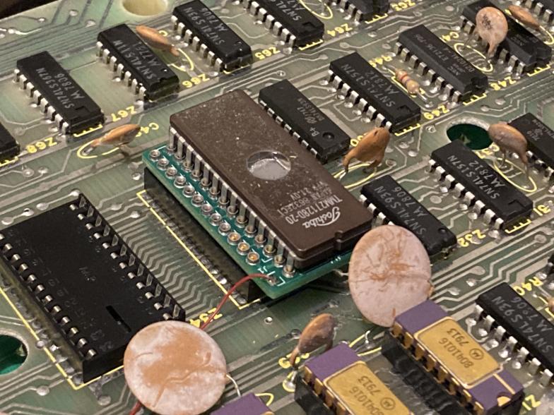
Using a single 27256 EPROM
Click to Enlarge
- To use install single 27256 EPROM in your 16K Model I follow these instructions written by Matt Boytim. You may need the referenced CPART file or the referenced FF2K.BIN file.
- The Dutch TRS-80 group also has a writeup on the same topic, found at https://trs80.nl/hardware/m1eprom/.
- Jurgen Bussert has also written up an article for both a 27256 and a 27128, which can be found at https://www.buessert.de/Technik/Museum/TRS-80/M1/ROM/english.htm. He has also developed a small PCB which will do most of the hard work. Unlike other solutions, the ROM does not need to be scrambled to use this solution. Anyone interested in the board should reach out to him by visiting his impressum page.
One point of note: You may need to verify that the motherboard does not have a solder bridge between Pin 7 and Pin 18 of ROM A. Some boards might have this. This bridge will prevent the EPROM from working.
Model I (With an Adapter)
The above technique uses a larger 27256 EPROM and scrambles the contents to simplify the wiring and installation. This is good approach but inconvenient if you got the scrambling wrong or otherwise want to reprogram the EPROM because you need to completely undo the redo the mods.
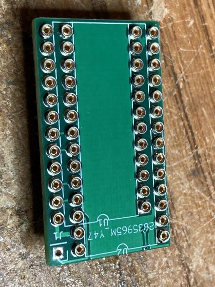
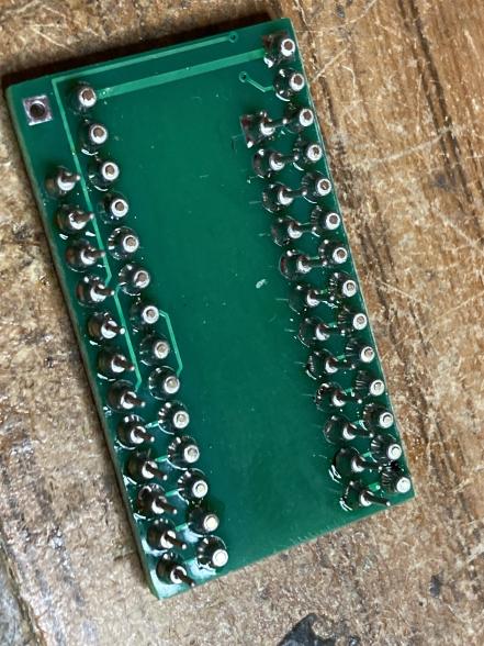
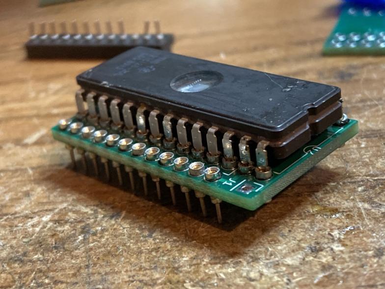
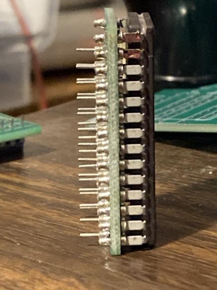
Matt Boytim has also developed some EPROM to TRS-80 adapter PCB’s to allow use of a 27128 EPROM and further simplify the installation. Two models are available:
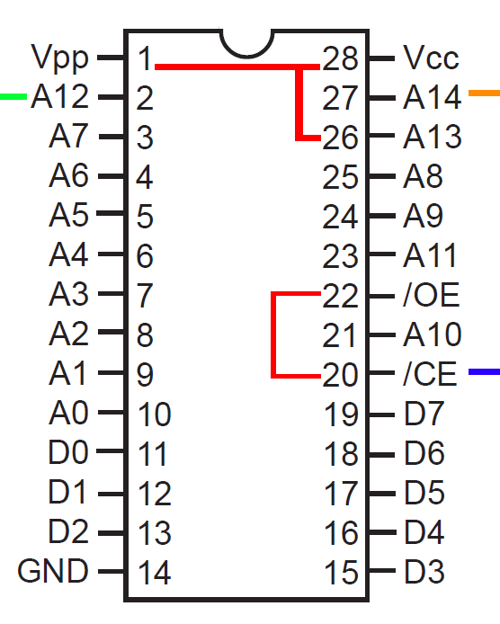
- A model which supports a single 12k image for a Model I but can also be used in replace an 8k ROM and select one of two 8k images. This is because the 16k EPROM requires one extra address line than is on the Model I ROM socket or 8k ROM socket. For the Model I this extra address is wired to A13 but in 8k ROM applications this extra address line can be connected low or high to select an image stored in the lower half or upper half for the EPROM. The adapter PCB has pads for a pullup resistor for A13 and a 2-pin header to connect A13 to ground (with a shorting block). For the Model I the pullup is not installed and A13 is just connected to the non-ground pad of the 2-pin header. For the 8k ROM application the pullup resistor and 2-pin header are installed such that with the shorting block installed the lower half image is used and without the shorting block installed the upper half image is used. An example of where this might be used for an 8k ROM replacement is the Model 4 gate array ROM B/C for the FreHD autoboot ROM or Frank Durda’s XROM. You can download that here.
- A model which is for the Model I only and supports selecting between a 12k image and 4k image, which for example might be Level 2 BASIC and Level 1 BASIC, or Level 2 BASIC and a diagnostic ROM. To support the swapping two XOR gates are used to conditionally invert address lines A13 and A12, and has a pullup resistor and 2-pin header to select using a shorting block. You can download that here.
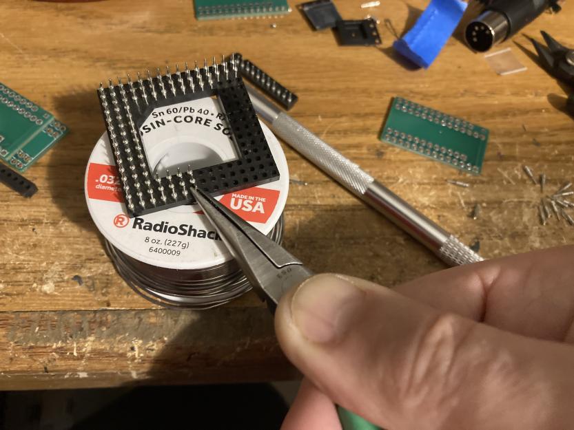
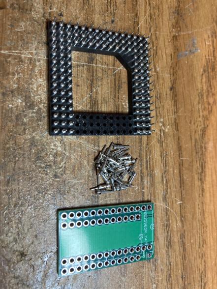
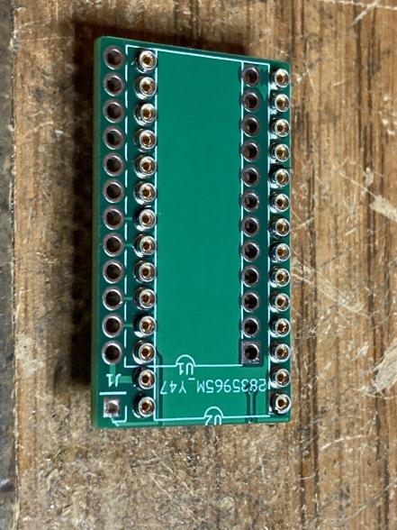
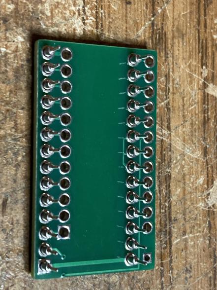
There are other adapter PCB’s with similar function but what is unique about these designs is they use machine socket pins for the module pins and the EPROM socket which make them very low profile and very compact. Conesequently the assembly procedure involves the removal of the pins from machine sockets and installing the individual pins in the adapter PCB. The detailed assembly instructions will make this more clear.
The assembly for both models is essentially the same and is pretty simple:
One note before we start … The connections for 2-15, 3-14, 4-13, 5-12 on the X3/Z3 shunt are for RAM, and this has nothing to do with that … so leave those unchanged. The picture should NOT be your guide; that was a picture from a single system which may be different than yours.